Reader Control
Order Number: M705
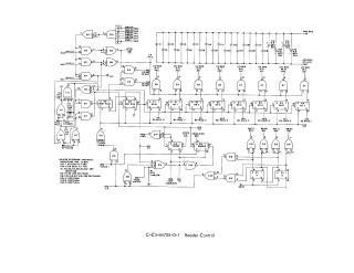
Summary
This document is a technical schematic for a "Reader Control" circuit board. It illustrates the logic gate architecture, including integrated circuits (DEC 7400-series chips) and control signal routing for an input/output (I/O) bus system. Key components of the schematic include:
- Logic Gates: A complex array of AND, OR, NAND, and flip-flop gates (such as E1 through E18) that manage data flow and read operations.
- I/O Bus Interface: A series of inputs labeled RD 0 through RD 7, indicating an 8-bit bus architecture for reading data.
- Power and Filtering: The design incorporates numerous capacitors (C1–C22) for signal decoupling and power stabilization.
- Control Signals: The circuit processes external commands such as "Initialize," "RDR Run," "Shift," and "Stop Complete," which coordinate the timing and state of the reader mechanism.
- Connectivity: The diagram details various test points (T.P.), power requirements (+5V), and specific input/output pins for integration with a larger computing system.
Site structure and layout ©2025 Majenko Technologies