Rs-c-g209 Memory Selector
Order Number: XX-XXXXX-XX
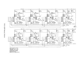
Summary This document is a technical schematic for a Memory Selector circuit. It displays two identical rows of transistorized switching stages, each utilizing DEC 2894-3 transistors and T-2051 transformers. The circuit is designed to handle multiple input signals (labeled A and B) and route them through diode-coupled logic networks. Key technical specifications provided at the bottom of the diagram note that, unless otherwise indicated, the system uses 100 MMFD capacitors, 1/4 W 5% resistors, and D-664 diodes. The circuit is powered by a dual-voltage rail configuration (+10V and -15V).
Site structure and layout ©2025 Majenko Technologies