Vfo Clock B410
Order Number: XX-XXXXX-XX
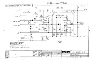
Summary This document is a technical schematic for the "VFO Clock B410," produced by the Digital Equipment Corporation in 1969. The diagram details the electronic circuit design, including the arrangement of transistors (Q1–Q4), various diodes (D1–D25), capacitors, and resistors. It specifies power inputs for +10V, -6.2V, -5.6V, -6.8V, -2.1V, and -15V, along with connections for control and trigger inputs. The document includes a conversion chart for the transistors and diodes used in the circuit, noting that unspecified resistors are 1/4W, 5% tolerance, and capacitors are .01 MFD, 100V, 20% unless otherwise marked.
Site structure and layout ©2025 Majenko Technologies