PDP.9
Order Number: XX-38D61-63
This document details the architecture, instruction set, and components of the PDP-9 computer.
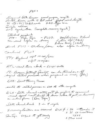
System Overview: The PDP-9 is a general-purpose computer featuring an 18-bit word length and a 1us memory cycle time. It supports single addressing and comes with 8K (or 8192) words of memory.
Registers and Memory: Key registers include the 18-bit Accumulator (AC), Memory Buffer (MB), 15-bit Memory Address (MA), Program Counter (PC), Instruction Register (IR), and a 1-bit Link (L) for arithmetic extensions. The system supports Two's complement and One's complement arithmetic. Main Memory is a 2.5D organized core memory (MC 70B) with an 8K capacity, utilizing a read-modify-rewrite cycle. Control Memory is read-only, pre-wired, and contains 64 (octal) addressable locations, each holding 36 bits (30 command, 6 address).
Peripherals and I/O: Standard peripherals include Paper Tape Reader/Punch (PC02/PC03) supporting alpha or binary modes, a TTY Keyboard (10 chars/sec I/O), and a Real-Time Clock (RTC) with a 60 cps counter. The system features a Program Interrupt Facility (PI) for peripheral readiness and Direct Memory Access (DMA). A Data Channel (DCH) provides medium-speed transfer for peripherals, particularly from Dee Tape.
Instruction Set: The document outlines various instructions:
- Arithmetic:
ADD(addition with end-around carry),TAD(Two's complement add). - Logic:
AND(masking/extracting),XOR. - Data Transfer:
DAC(deposit AC),LAC(load AC),DZM(deposit zero). - Flow Control:
JMP(jump),JMS(jump to subroutine),ISZ(increment and skip if zero),SAD(skip if accumulator different). - I/O Operations:
IOTcodes for device selection and control. - System Control:
CAF(clear all flags),ION(enable interrupt),IOF(disable interrupt),KSF(skip on keyboard flag),KRB(read keyboard buffer),LAW(load AC with word). - Addressing Modes: Indirect addressing (I*) and Auto-indexing (memory locations 10-17).
Core Operations: The document describes the Fetch Cycle, detailing the timing and data flow between registers for instruction retrieval.
Circuit Elements: It includes diagrams and descriptions of fundamental digital logic gates (Diode AND/OR, NAND/NOR), Flip-Flops (Jam Flip-Flop), delay networks (Tapped Delay Line, Single Shot), and pulse amplifiers. These elements illustrate the underlying hardware implementation of the PDP-9's logic and timing.
Site structure and layout ©2025 Majenko Technologies