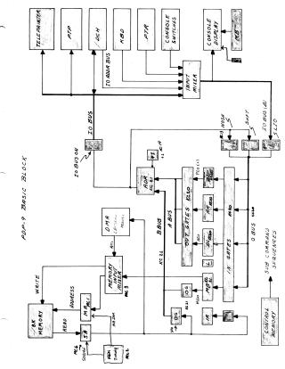
PDP-9 Basic Block
Order Number: XX-3339B-1E
This document is a collection of technical diagrams, charts, and textual explanations primarily detailing aspects of the PDP-9 computer system and a specific logic component, the B-131 Adder.
The PDP-9 related content includes:
- Basic Block Diagram (Page 1): An architectural overview showing key components like memory, I/O bus, internal data buses (BBUS, A BUS), control logic, and various peripherals (Teletypewriter, PTR, KBD, Console Display).
- Programming & Timing (Pages 2, 3, 21, 23, 24): Examples of program execution (DEC Tape Reading) with memory/register states, detailed timing diagrams for main memory operations (e.g., CLK, MAJAM, WRITE), and specific operational timings for interrupts, DBR, and real-time clock.
- Memory Reference Instructions (Page 10): A demonstration program listing mnemonics and their encoded values for common memory reference instructions like LAC, AND, ADD, JMP, and TAD.
- Instruction Logic Diagrams (Pages 11-20): Detailed logic schematics illustrating the data paths and control signals for implementing individual PDP-9 instructions (e.g., LAC, AND, SAD, ADD, XOR, JMP, ISZ, TAD), showing register transfers and gate operations via the A and B buses.
- Tape Drive Operation (Pages 25-30): Tables detailing bit patterns ("W1 W2...W9") for various tape marks (e.g., Reverse End, Interblock Sync, Data Mark, FWD End), describing the logic for tape travel and synchronization.
The document also provides an in-depth analysis of the B-131 Adder circuit and other logic components:
- Adder Block Diagram & Logic (Page 33): A high-level view of the Adder, comprising a Summing Network and a Carry Network, along with fundamental rules for sum and carry generation.
- Summing Network Details (Pages 34-36, 43): Textual explanations of the transistor-level operation, current flow, and voltage potentials that determine the sum output, accompanied by a truth table detailing input combinations, transistor states, and resulting sum.
- Carry Network Details (Pages 37-41, 43): Textual descriptions of the carry logic, including transistor conduction, voltage levels for carry output, and a truth table showing inputs, Q10/Q11 states, and carry output. Detailed current and voltage tables further illustrate the circuit's behavior.
- Flip-Flop Schematics (Pages 31-32): Circuit diagrams for the S202 F.F. and B213 F.F.
- Simplified Logic Gates (Pages 5-9): Diagrams showing simplified representations of basic logic gates (inputs feeding into a transistor symbol).
- Detailed Adder Schematics (Pages 42-43): Transistor-level circuit diagrams of the B-131 Adder, showing all components and connections.
Site structure and layout ©2025 Majenko Technologies