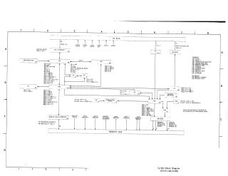
System Block Diagram
Order Number: XX-54AB1-8E
This document provides a comprehensive hardware specification for a digital computer system, detailing its architecture, control logic, and operational sequences across multiple functional units. It begins with a high-level system block diagram showing the interconnection of the I/O Bus, CPU components (Instruction Register, Program Counter, Arithmetic Register, Memory Buffer, etc.), and Memory. Subsequent sections delve into the detailed implementation of:
- Instruction Processing: Covering instruction decoding for various instruction types (arithmetic, logical, data transfer, control flow, I/O), along with the sequential steps of Instruction, Address, Fetch, Execute, and Store cycles.
- CPU Registers & Control: Dedicated sections illustrate the internal structure and control logic for critical registers such as the Program Counter (PC), Instruction Register (IR), Memory Buffer (MB), Memory Address (MA), Arithmetic Register (AR), Multiplier Quotient (MQ), Shift Counter (SC), and Floating Exponent (FE), including their shift connections and special inputs.
- Memory Management: Outlining memory addressing, control signals (read/write, clocking), the Memory Buffer Interface, address relocation via the Relocation Adder and Register, and memory protection mechanisms.
- Arithmetic & Logic Operations: Providing detailed logic for both fixed-point and floating-point arithmetic operations (add, subtract, multiply, divide, exponent calculation, normalization), and various logical and data transfer instructions.
- Input/Output Operations: Describing Input/Output Transfer (IOT) instructions and the intricate control logic for specific peripheral devices, including the Console, Teletype (TTY), Paper Tape Reader (PTR), Paper Tape Punch (PTP), and Card Reader (CR).
- System Control: Explaining the Key Cycle for manual system interactions, Program Interrupt (PI) handling, and the Central Processor Alarm (CPA) interface.
The document primarily utilizes detailed logic diagrams, complete with signal types, polarities, and gate-level implementations, to illustrate the precise flow of data and control signals throughout the system.
Site structure and layout ©2025 Majenko Technologies