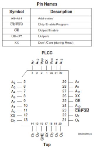
Pin Names
Order Number: XX-A4136-45
This document provides information about the pin names and their functions for a component in a PLCC (Plastic Leaded Chip Carrier) package. It includes a table that defines various symbols such as A0-A14 (Addresses), CE/PGM (Chip Enable/Program), OE (Output Enable), O0-O7 (Outputs), and XX (Don't Care during Read). Below the table, there is a detailed 32-pin PLCC pinout diagram, illustrating the assignment of each pin number (1-32) to specific functions like address lines (A0-A14), output lines (O0-O7), control signals (CE/PGM, OE), power (Vcc, Vpp), ground (GND), and unspecified pins (XX).
Site structure and layout ©2025 Majenko Technologies