Data Buffer & Status
Order Number: M7104-0-1
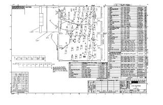
This document is a set of schematics for a Digital Equipment Corporation (DEC) system, specifically detailing the Data Buffer and Status Register functionalities. It includes various logic diagrams illustrating the interconnections of integrated circuits (ICs) and other electronic components. The schematics are organized by function, with separate sheets for "Data Buffer Control," "Data Buffer," "Omnibus Drivers," "Omnibus Receivers," and "Status Register Error Detect." Each schematic shows input and output signals, component designators (e.g., 74LS74, 74LS08), and their corresponding pin numbers. The document also contains a parts list for each section, specifying quantities, descriptions, and part numbers. The drawings are dated and contain revision information, indicating a design and development process.

Site structure and layout ©2025 Majenko Technologies